Introduction
A thin film can be defined as any material with a thickness ranging from a fraction of a nanometre (nm) to a few microns (μm).
The manufacture of thin films onto various substrates is vital to high-tech industries. The deposition of optical coatings, the production of highly integrated chips on silicon wafers, the manufacture of thin film solar cells and batteries, and even thin film drug delivery systems in the pharmaceutical industry are all examples. And all are manufactured in strictly controlled clean room environments.
Thin films are also needed for more general purpose packaging industries, such as kitchen film (“cling” film) and any other manufacturing business requiring some form of protective or resistive coating that brings useful features to a final product. Products exhibiting special optical or electrical properties are good examples.
In all of these applications, precise control of film thickness is of paramount importance, particularly for microelectronic and optical components which have to deal with sub-nanometre control limits and very tight specifications. But even for a standard packaging business, careful control of the thickness of a packaging material can be important. After all, no-one wants to see an item as common as kitchen cling film that is uneven in thickness and uniformity!
Thin Film Reflectometry
One way to determine the thickness of a thin film employs the interference properties of white light transmitted through the film and then reflected back from an underlying substrate in direct contact with the film. This technique is referred to as Thin Film Reflectometry or Reflectometric Interference Spectroscopy.
With this method, a white light source is incident on a thin film sample at a certain angle θ. Some of the light reflects back from the first (top) surface of the film and some light penetrates through the film and is reflected back from the film-substrate interface. This is shown schematically in these two images, courtesy of Semantic Scholar and used with permission:
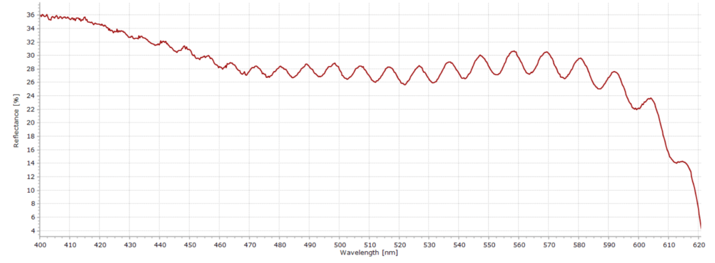
The result is a spectrum with a series of oscillations (called fringes) that correspond to the interference pattern that is generated. A typical example can be seen here:
Provided we know the refractive index of the material under test, and if we count the number of peaks (or the number of valleys) in this interference spectrum within a given wavelength range, we can determine the thickness d of the thin film according to the following expression:
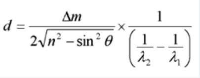
Δm is the number of interference maxima (or minima) in the spectrum, λ1 and λ2 represent the wavelength range of the measurement and n is the refractive index of the material (which is shown as N2 in Figure 1 above).
Experimental Setup
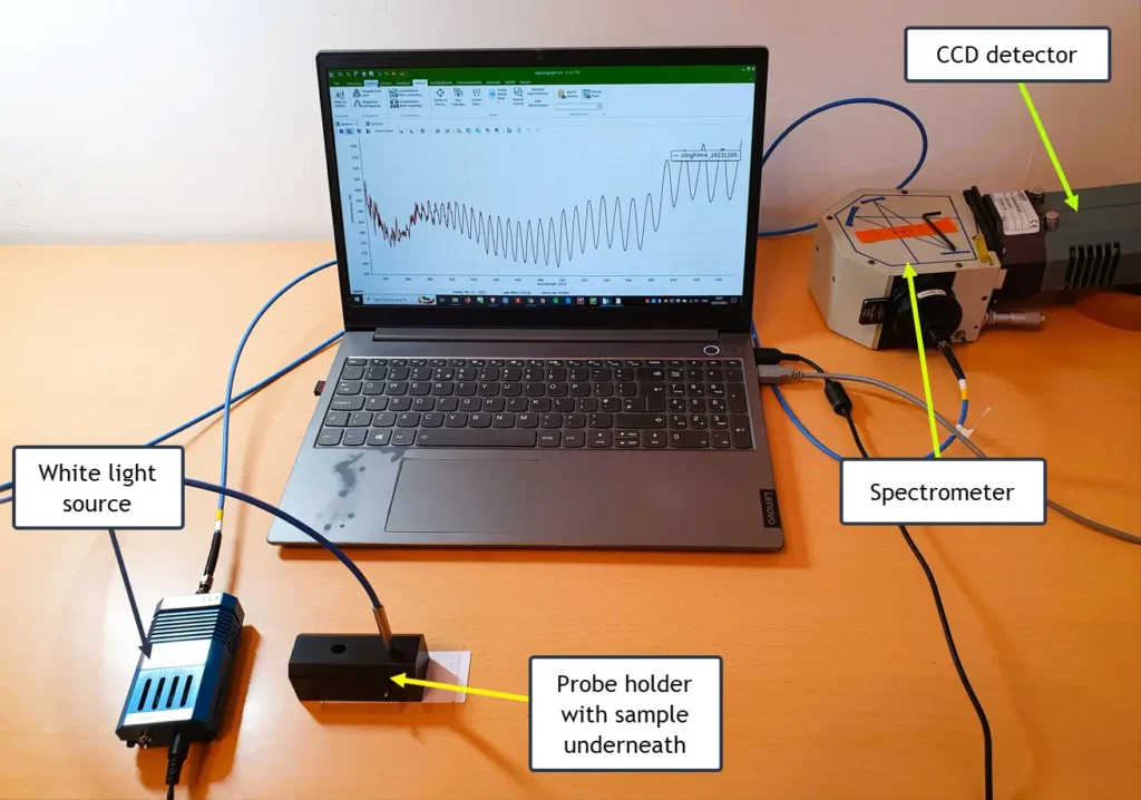
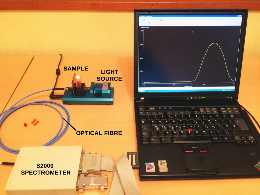
The experimental setup for a thin film reflectometric measurement is very similar to the arrangement used in two earlier posts on Diffuse Reflectance Spectroscopy and Fruit & Veg spectroscopy.
The experiment consists of a white light source, in this case a LS-1 tungsten halogen lamp from Ocean Insight, a reflection probe (Ocean Insight), and a small spectrometer. The two earlier posts used an S2000 fibre-optic spectrometer. This time we are using the MS125 1/8m Czerny-Turner spectrometer with an iDUS 420 CCD detector.
Fibre-optic spectrometers and light sources such as these are regularly found second hand on eBay at reasonable cost.
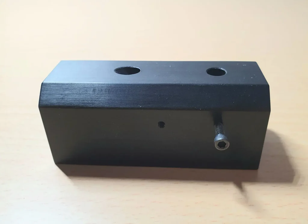
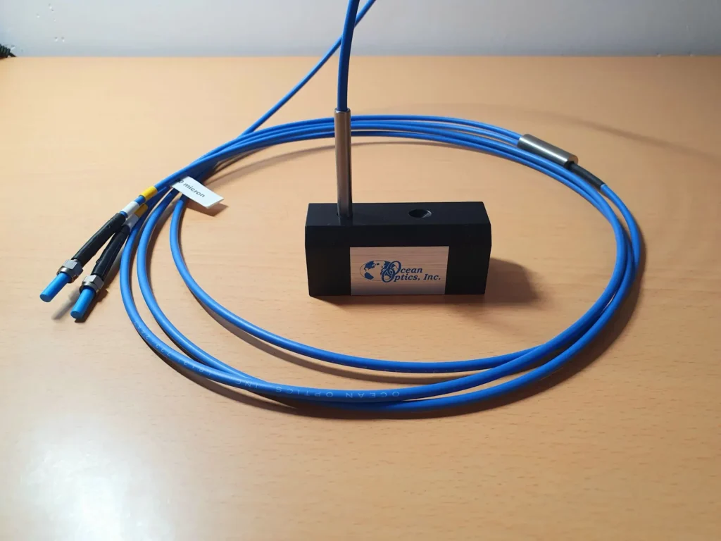
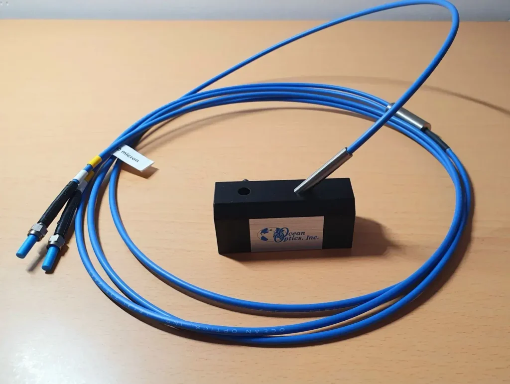
The central component of this experiment is the reflection probe fibre. Its function is to transmit broad band white light onto the sample through one bundle of fibres and then to collect the reflected light and return it via a receiving fibre. This reflected light originates from the two interfaces: air/film and film/substrate (refer to Fig.1).
Fibre optic probes for measuring reflectance properties of surfaces, and any coatings deposited on these surfaces, are also referred to as splitter cables. The cable splits into two sections, one section directing incident light onto the sample and the other catching reflected light from the sample and sending it to the spectrometer.
Typical probes usually consist of 5-6 single illumination fibres arranged around a central fibre that is used to collect the reflected light.
A generalized schematic diagram is shown here…
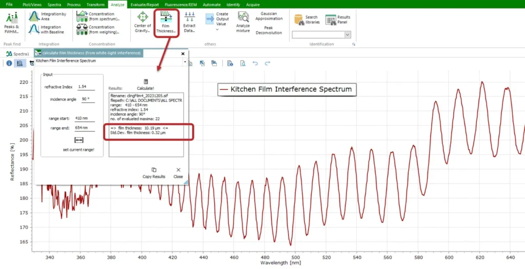
In order to perform the relevant calculations that determine the thickness of a thin film sample we can take advantage of a very useful feature in Spectragryph. Some of the main aspects of the Spectragryph software package were described recently in this post. Here, we focus on the Analysis Menu in the software which contains a practical calculation routine for estimating film thickness from a measured interference fringe pattern.
An example calculation is provided here, which has estimated the thickness of a sample of kitchen wrapper film to be about 10.2 μm, with a standard deviation of 0.32 μm. This value agrees well with the nominal thickness reported by film manufacturers as well as literature values.
Several Results
- Sunglasses
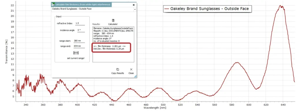
Good quality sunglasses usually have some form of anti-reflection coating applied during manufacture. This also acts as a scratch resistant protective layer. Here is the result from the film thickness measurement of a pair of Oakley sunglasses, indicating an anti-reflection film thickness of around 2 μm – so a relatively thin coating.
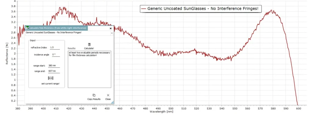
On the other hand, below is the result from a cheap pair of generic sunglasses. No interference fringe spectrum is produced. Clearly, this cheaper pair do not have any applied anti-reflection coating.
- Antistatic Bags
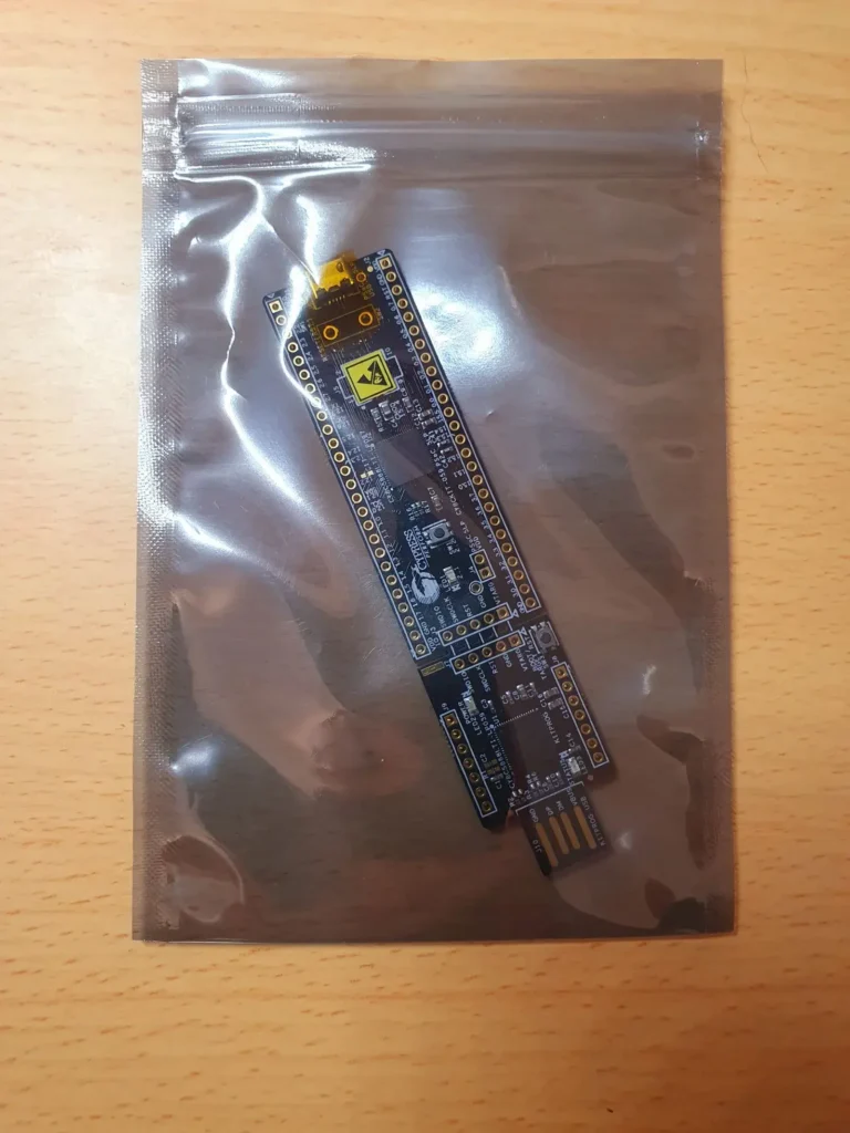
Antistatic bags are often used for protecting sensitive integrated circuits and other electronic components from accidental electrostatic discharge during storage and handling. These discharges can destroy sensitive CMOS and other IC’s before they are even used.
The bags are often dark metallic grey or silver in colour. This is due to a thin film of conductive aluminium particles deposited on the plastic, which is usually polyester – polyethylene terephthalate, PET. This metallic film is designed to dissipate the build up of any electrostatic charge when components are being handled before being soldered onto a circuit board.
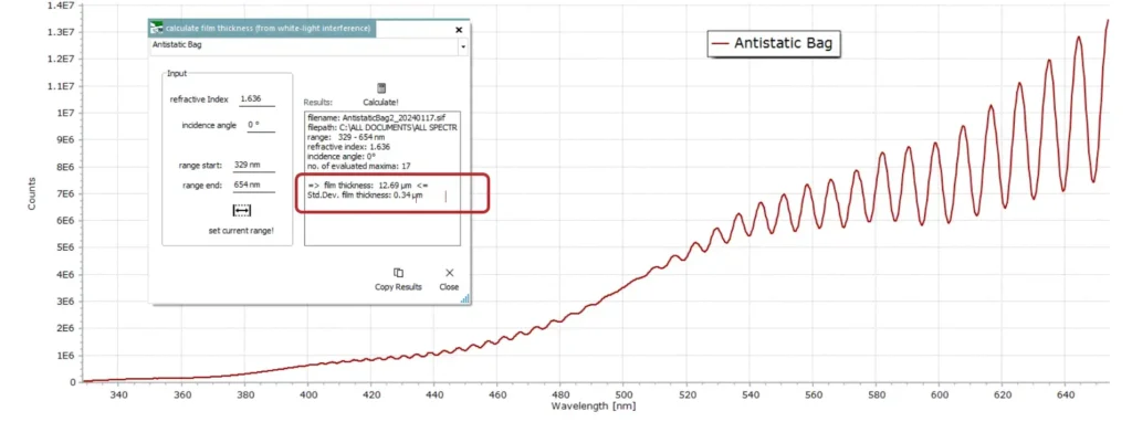
Here is the result of a thin film measurement from the surface of one of these antistatic bags.
The interference fringe pattern in this example is very well defined and the thickness of the antistatic layer is determined to be 12.7 μm, from 17 fringes observed in the spectrum, with a standard deviation of 0.34 μm.
- Eyeglasses
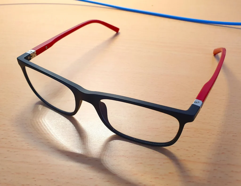
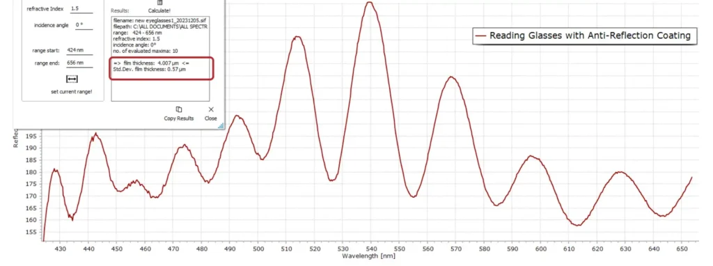
Eyeglasses can come with or without an anti-reflection coating. Shown above is my own pair of reading glasses that have such a coating. Here is the result:
The calculated thickness of this anti-reflection is about 4 μm.
- Food Packaging Films
Films used for food packaging and for keeping opened food in your fridge often come in two types. The type that clings and sticks to food containers and plates is made from PVC (polyvinyl-chloride); the type that doesn’t stick too well is made from LDPE (low density polyethylene). So the next time you are out shopping for some cling film, check the labelling before you buy! 😉
Here is the result for a typical kitchen cling film sample, using a generally accepted value for the refractive index of PVC film of 1.54. Estimated film thickness is about 8 μm.
- Coatings for Optical Instruments
Virtually all good quality lenses used in cameras, telescopes, microscopes, binoculars and so on have thin film “anti-reflection” and other specialized coatings deposited on the lenses during manufacture. These coatings help to minimize internal “ghost” reflections within the body of the lens. The coatings are usually vacuum deposited on the lens glass and give coated lenses their characteristic green, pink or blue colour when observed in reflected light.
Manufacturers tend to be highly secretive regarding their own “recipes” for vacuum depositing different coatings on optical components. But as a general rule, dielectric and metallic materials are used consisting of magnesium fluoride (MgF2), the oxides of titanium, silicon and aluminium, tantalum pentoxide (Ta2O5) and hafnium oxide (HfO2) in alternating thin layers.
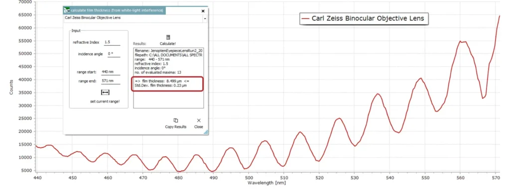
Here is the result of a measurement I made recently on my old pair of Zeiss binoculars (Carl Zeiss Jenoptem 10 x 50’s). The result I obtained of 8.5 μm represents the total film thickness from several different coatings. Each individual coating typically has a thickness of 1-2 μm so the lens has undergone several thin film vaccum coating deposits during manufacture.
- Laptop Screen
Laptop displays and our smartphones also have some form of thin film coating on them, whether it is a capacitative electrode structure across the whole screen used with touch-sensitive displays, or an anti-glare coating for regular screens.
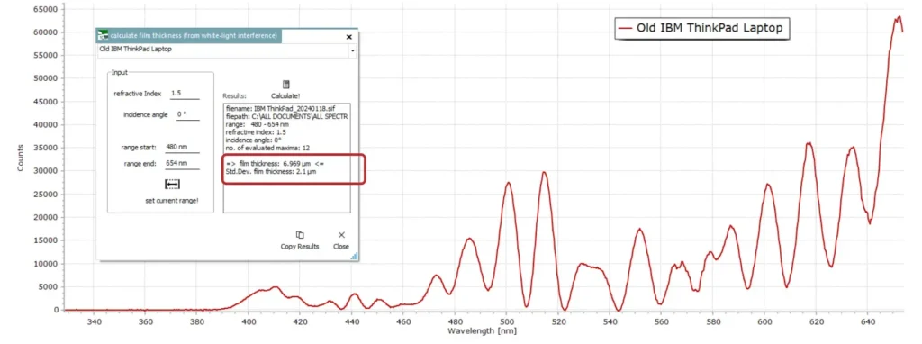
Here are the results for my old legacy IBM Thinkpad laptop, estimating a film thickness of 7 μm, but with an uncertainty in this estimate of 2 μm. This is most probably due to the irregularity in the width of some of the interference fringes which is evident from the spectrum:
- Soap Bubbles!
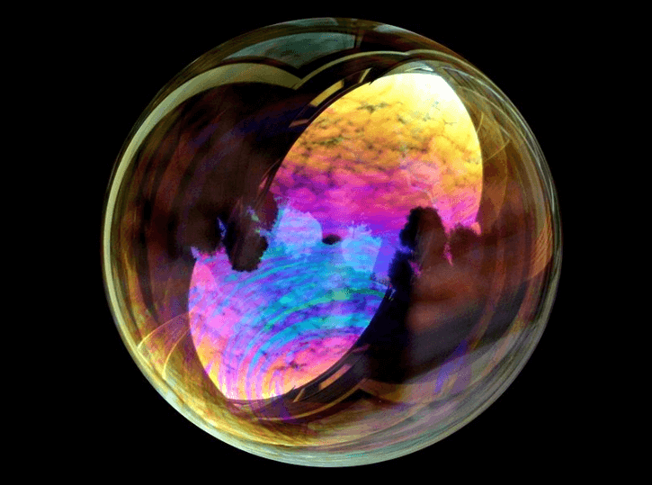
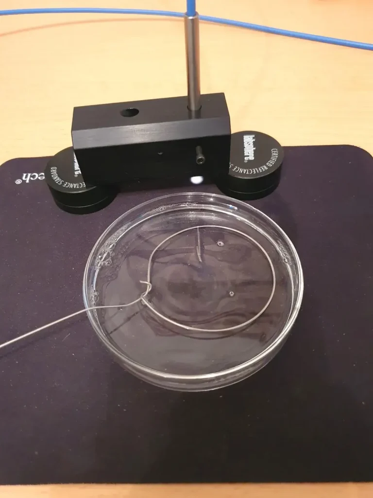
As kids, we have all played with blowing soap bubbles at one time or another. This final example, therefore, is an attempt to measure the thickness of such films produced by the usual loop of wire and some soap solution – washing up liquid in this case.
One of the “technical” challenges, of course, is the limited lifetime of soap films (typically only several seconds that as kids we know only too well). So the interference fringe spectrum, upon which these calculations are based, must be recorded within this timeframe before the soap film suddenly breaks!
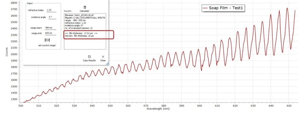
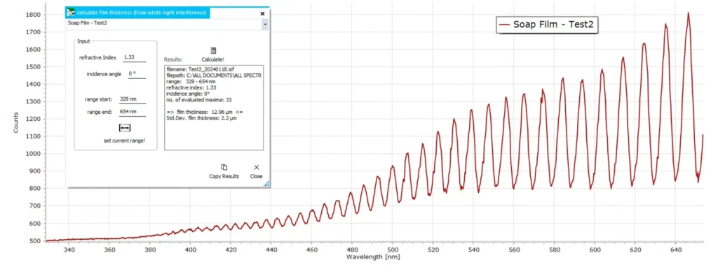
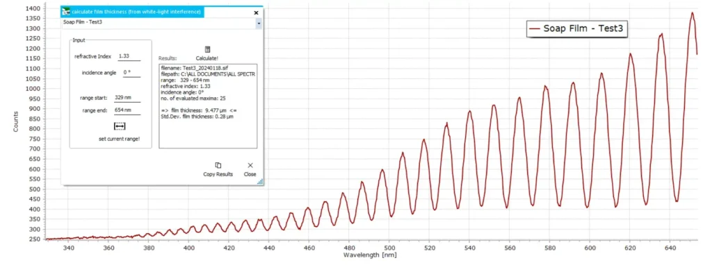
Below are several results of soap film thickness determinations…
The measured film thicknesses of the soap films in the above three examples vary considerably. This is very likely due to surface tension variations within the film since it is dynamically changing during the lifetime of the film. This affects film thickness, which therefore varies over time – until the soap film finally bursts, of course!
Conclusions
In conclusion, a spectroscopic technique, such as Reflectometric Interference Spectroscopy described here, offers a quick, practical and non-destructive method to estimate he thickness of thin films for a wide range of different materials.






Very interesting! 🙂
Awesome! Just checked an electrostatic bag, and wasn’t sure where that oscillation came from, now I have a clue.